


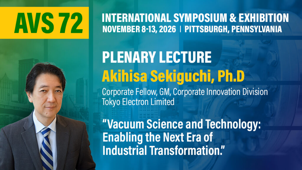
Monday, November 9, 2026 | 8:30 a.m.
“Vacuum Science and Technology: Enabling the Next Era of Industrial Transformation”
Abstract
As the world enters a new era shaped by artificial intelligence, advanced semiconductor technologies, sustainable energy solutions, and digital transformation, vacuum science and technology continue to serve as essential foundations for innovation. From enabling atomic-scale precision in semiconductor fabrication to advancing breakthroughs in materials science, quantum technologies, and frontier surface science, the vacuum science community has played a pivotal role in transforming scientific discoveries into scalable industrial solutions.
This plenary presentation will examine how ongoing advances in vacuum engineering, process technologies, and intelligent manufacturing systems are addressing some of the most critical challenges facing industry today, including device scaling, heterogeneous integration, and increasingly complex production architectures. The discussion will highlight how vacuum-enabled platforms are evolving to enhance manufacturing performance, accelerate technology roadmaps, improve operational productivity, and support sustainability objectives through greater resource efficiency and reduced environmental impact.
As industries push the boundaries of precision, complexity, and sustainability, vacuum science and technology will remain an indispensable catalyst for innovation, enabling the technologies and manufacturing ecosystems that will define the next era of industrial transformation.
Biography
Dr. Akihisa (Aki) Sekiguchi currently serves as Senior Vice President & General Manager, U.S. R&D, Tokyo Electron America, Inc. Aki is responsible for planning and executing the worldwide alliance strategy for the division, including programs related to AI, quantum computing, and advanced CMOS logic development.
He is currently on SEMI`s Board of Industry Leaders and is a member of the CTO Forum representing TEL.
In previous roles, he has led Corporate Marketing and Corporate Technology Development at TEL as the VP and GM.
Prior to joining TEL in 2007, he worked for IBM Microelectronics Division for 17 years. As part of the Semiconductor Research and Development Center, he worked on the development of FEOL, MOL, and BEOL process and equipment that enabled IBM`s DRAM and SOI-based logic technologies. During his last three years with IBM, he was responsible for process technology transfer from IBM to Sony (used in PlayStation 3).
Aki earned his Ph.D. in Applied Physics from Columbia University, M. Eng. and B.S. in Engineering Physics from Cornell University, and an MBA in Finance from the Stern School of Business (New York University) while working for IBM. His doctoral thesis was on experimental plasma physics for thermonuclear fusion.