

x-twitter
#AVS72
AVS-72 Website logo 207x46 v2AVS-72 Website logo 207x46 v2
avslogo_blue_92x94avslogo_blue_92x94
  • Overview
    • Greetings & Introduction
    • Venue & Location
    • Organizing Committee
      • Meet Mark Losego – AVS 72 Program Chair
      • Program Chairs and Committee Members
    • AVS Code of Conduct
    • Awards
      • 2026 AVS Awardees
      • Awards Ceremony
      • Travel Grants
    • Manuscripts
    • Presentation Guidelines
    • Promote AVS 72: How to Help
      • Promotional Tips and Tools
      • AVS 72 PowerPoint Template (PPT)
      • AVS 72 Print Ad (PDF)
      • AVS 72 Customizable Flier (PPT)
      • AVS 72 Print Banner (jpg)
      • AVS 72 Banner Ad Late News Call 350 x 350 (jpg)
      • AVS 72 Banner Ad Late News Call 1200 x 675 (jpg)
      • AVS 72 Banner Ad 300 x 250 (jpg)
      • AVS 72 Banner Ad 400 x 400 (png)
      • AVS 72 Banner Ad 600 x 90 (png)
      • AVS 72 Banner Ad 1200 x 675 (jpg)
      • AVS 72 Banner Ad Call 1200 x 675 (jpg)
      • AVS 72 Banner Ad Plenary 1200 x 675 (jpg)
      • AVS 72 PowerPoint Banner Ad 1920 x 190 (png)
      • Why Attend Print Ad (PDF)
      • Why Attend Video
    • Press Registration Form
    • Photo Gallery
  • Technical Program
    • Symposia
      • Divisions & Groups
        • 2D Materials (2D)
        • Advanced Surface Engineering (SE)
        • Applied Surface Science (AS)
        • Biomaterial Interfaces (BI)
        • Electronic Materials and Photonics (EM)
        • Magnetic Interfaces and Nanostructures (MI)
        • Manufacturing Science and Technology (MS)
        • Nanoscale Science and Technology (NS)
        • Plasma Science & Technology (PS)
        • Spectroscopic Ellipsometry (EL)
        • Surface Science (SS)
        • Thin Film (TF)
        • Vacuum Technology (VT)
      • Focus Topics
        • Actinides and Rare Earths (AC)
        • Advanced Packaging (PK)
        • Advances in EUV Lithography (EUV)
        • AI/ML Autonomous Experimentation for Thin Films Processing (AIML)
        • Chemical Analysis and Imaging of Interfaces (CA)
        • Light Sources Enabled Science (LS)
        • Materials and Innovations for Fusion Energy (FUS)
        • Multifunctional and Hybrid Microsystems (MC)
        • Quantum Science & Technology (QS)
        • The Future of Temperature Sensing (TS)
      • Mini-Symposia
        • Advanced Microelectronic Materials and Devices (AM)
        • Atomic Scale Processing (AP)
        • Advances in Battery Engineering, Interface Design, and Characterization (BT)
    • Special Sessions & Events
      • 5K Run
      • AVS Member Center
      • AVS Publications Author & Reviewer Appreciation
      • Career Center & Job Fair
      • Plenary Lecture
      • Special Symposium: A Celebration of Gary W. Rubloff’s 50+ Years in Science (GWR)
      • AVS Quantum Science Workshop
      • Biomaterials Plenary (BP)
      • Exhibitor Technology Spotlight (EW)
      • Nanoscale Science and Technology Plenary (NSP)
      • Science Educators Workhop
      • Tutorials
      • Undergraduate Posters (UN)
    • Abstract Book (PDF)
    • Technical Program (PDF)
    • Technical Program & Online Scheduler
    • Mobile App
    • Short Courses
    • Submit Abstract
    • Copyright Agreement
  • Housing & Registration
    • Attendee Hotel Reservations
    • Exhibitor/Staff Hotel Reservations
    • Symposium Registration | Rates | Hours
    • Housing Rates | Travel
    • Accessibility
    • Directions | Parking
    • International Visitor Information
    • International Visitor FAQ
    • Things to Do
    • Maps
      • David L. Lawrence Convention Center
  • Exhibit
    • Exhibit Information & Opportunities
    • Exhibit & Sponsor Form (Online)
  • Sponsors
    • Major and General Sponsors
    • Division, Group, and Focus Topic Sponsors
    • Sponsorship Opportunities

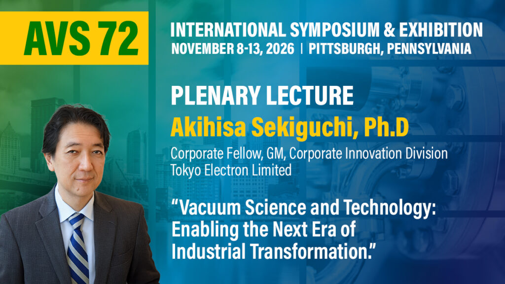
Plenary Lecture

Home Plenary Lecture

Monday, November 9, 2026 | 8:30 AM
David L. Lawrence Convention Center
Ballroom BC

“Vacuum Science and Technology: Enabling the Next Era of Industrial Transformation”

Abstract

As the world enters a new era shaped by artificial intelligence, advanced semiconductor technologies, sustainable energy solutions, and digital transformation, vacuum science and technology continue to serve as essential foundations for innovation. From enabling atomic-scale precision in semiconductor fabrication to advancing breakthroughs in materials science, quantum technologies, and frontier surface science, the vacuum science community has played a pivotal role in transforming scientific discoveries into scalable industrial solutions.

This plenary presentation will examine how ongoing advances in vacuum engineering, process technologies, and intelligent manufacturing systems are addressing some of the most critical challenges facing industry today, including device scaling, heterogeneous integration, and increasingly complex production architectures. The discussion will highlight how vacuum-enabled platforms are evolving to enhance manufacturing performance, accelerate technology roadmaps, improve operational productivity, and support sustainability objectives through greater resource efficiency and reduced environmental impact.

As industries push the boundaries of precision, complexity, and sustainability, vacuum science and technology will remain an indispensable catalyst for innovation, enabling the technologies and manufacturing ecosystems that will define the next era of industrial transformation.

Biography

Dr. Akihisa (Aki) Sekiguchi currently serves as Senior Vice President & General Manager, U.S. R&D, Tokyo Electron America, Inc.  Aki is responsible for planning and executing the worldwide alliance strategy for the division, including programs related to AI, quantum computing, and advanced CMOS logic development.

He is currently on SEMI`s Board of Industry Leaders and is a member of the CTO Forum representing TEL.

In previous roles, he has led Corporate Marketing and Corporate Technology Development at TEL as the VP and GM.

Prior to joining TEL in 2007, he worked for IBM Microelectronics Division for 17 years.  As part of the Semiconductor Research and Development Center, he worked on the development of FEOL, MOL, and BEOL process and equipment that enabled IBM`s DRAM and SOI-based logic technologies.  During his last three years with IBM, he was responsible for process technology transfer from IBM to Sony (used in PlayStation 3).

Aki earned his Ph.D. in Applied Physics from Columbia University, M. Eng. and B.S. in Engineering Physics from Cornell University, and an MBA in Finance from the Stern School of Business (New York University) while working for IBM.  His doctoral thesis was on experimental plasma physics for thermonuclear fusion.

Follow Us

Posts by AVS_Members

Key Dates

Major Awards Deadline:
March 31, 2026

Student Awards Deadline:
May 18, 2026

Abstract Submission Deadline:
May 18, 2026

Late News Abstract Submission Deadline:
September 14, 2026

Hotel Deadline:
September 30, 2026

Early Registration Deadline:
October 5, 2026


Contact

Yvonne Towse
Conference Administrator
125 Maiden Lane; Suite 15B
New York, N.Y. 10038
yvonne@avs.org


OverviewTechnical ProgramHousing & RegistrationExhibitSponsors
© 2026 AVS. All Rights Reserved.